Huawei Unveils Tau Scaling Law at ISCAS 2026, Proposing a New Rulebook for the Chip Industry

At the IEEE International Symposium on Circuits and Systems (ISCAS) in Shanghai, He Tingbo, Chair of Huawei's Scientist Committee and President of its Semiconductor Business Department, delivered a keynote titled "New Semiconductor Path in Practice."
In her speech, she introduced what the company calls the Tau (τ) Scaling Law, a principle that industry peers have already begun referring to informally as "Her's Law" in a nod to He Tingbo herself.
The problem Huawei faces today is clear. China's semiconductor industry has no access to ASML's EUV machines, which are used to produce the most advanced chip nodes. SMIC, the most capable domestic foundry, can only manage 7nm-class processes. Meanwhile, US and Taiwanese competitors have already moved to 2nm production. The Tau Scaling Law is the answer Huawei has chosen to overcome that constraint.
What Huawei is proposing is a "new law" for semiconductor development. It marks the first time a Chinese company has put forward a scaling law of industry-wide ambition, set against Gordon Moore's Law from 60 years ago.
A New Law That Challenges Moore's Law
Before unpacking the Tau Scaling Law, it helps to revisit Moore's Law itself.
Moore's Law is Gordon Moore's 1965 observation that the number of transistors on a chip would double roughly every two years. It became the principle that drove the semiconductor industry for more than five decades. Every company raced to make transistors smaller and smaller, from 90nm to 45nm to 14nm to 7nm to 3nm.
The problem is that by 2026, further transistor shrinking is reaching the limits of physics. Atomic dimensions impose hard ceilings. The cost per transistor, which used to fall consistently, no longer does. And the complexity of EUV machines means only ASML in the Netherlands can produce them, leaving the entire industry dependent on a single company in a single country.
The Tau Scaling Law proposes a different target. Instead of shrinking dimensions, the goal becomes shrinking time. The variable τ (tau) represents the time constant, which is the signal propagation delay inside a circuit. Put simply, rather than competing to build the smallest transistor, companies should compete to reduce how long a signal takes to travel through a chip.
Huawei's idea may turn out to be a defining moment for the chip industry. Shrinking dimensions requires EUV machines and fabs that cost hundreds of billions of dollars. Shrinking time, by contrast, can be done through architectural design. It is a problem of engineering rather than a problem of machinery.
LogicFolding and the 4 Levels of Co-Optimization
To make the Tau Scaling Law work in practice, Huawei has built a framework it calls "Multi-level Co-optimization," which tunes four layers of the system together to drive τ down as far as possible.
Level 1: Device Level
This is the deepest layer of physics. Huawei says it will optimize the resistance and parasitic capacitance of transistors so that signals travel faster within the device itself. It is a fix at the material and structural levels.
Level 2: Circuit Level
Huawei has introduced a new architecture called LogicFolding, which literally means "folding the logic circuit." The idea is to break the physical boundaries of conventional single-layer circuit layouts and "fold" the circuit upward, shortening the critical paths that signals must travel. This reduces both resistive and capacitive loading. The result is that transistor density and circuit performance increase at the same time.
To picture it, LogicFolding is like folding a sprawling Bangkok street map into a three-dimensional plan. You can travel from Bang Na to Lat Phrao faster, even though the underlying distance hasn't changed.
Level 3: Chip Level
This is where Huawei coordinates software, architecture, and silicon. By using fine-grained, workload-driven control over instruction and data flow, the company aims to boost system-level parallelism and efficiency, and to shorten end-to-end execution time.
Level 4: System Level
This level introduces a new interconnect protocol called UnifiedBus. It is the backbone that allows thousands of AI processors to share memory as if they were inside a single computer, rather than operating as a traditional cluster where each node has its own separate memory.
Systems built on UnifiedBus are called SuperPoDs. A SuperPoD is a massive AI cluster that links large numbers of Ascend NPUs to operate in unison. The flagship Atlas 950 SuperPoD connects up to 8,192 Ascend NPUs. The Atlas 960 SuperPoD, scheduled for 2027, will connect up to 15,488. The goal is to cut the communication latency that has long been the bottleneck of large-scale AI systems.
What is interesting about looking at chips through these four layers is that Huawei does not need to "win" at every level. As long as τ can be reduced at any one of them, the overall result improves. It is a way out of the trap of being forced to rely on EUV alone.
Why Do It Now?
To understand why Huawei is opening this front today, the story has to go back to 2019.
That year, Huawei was placed on the US Entity List. As a result, the company lost access to the world's most advanced manufacturing equipment, especially ASML's EUV machines, which are essential for chips below 7nm. SMIC, Huawei's main foundry partner in China, can only manage its N+3 process, which sits around the 7nm-class level. That is the process behind the current Kirin 9030.
Meanwhile, Apple uses TSMC to produce its A19 chip at 3nm and is already preparing for a 2nm chip. Nvidia and AMD are following the same path. The technological gap between Huawei and the rest of the world has widened every year since.
Huawei announced that over the six years since sanctions began, it has accelerated chip design and mass production, shipping 381 chips that span everything from smartphones to AI data centers — a figure also cited in coverage by Reuters and Nikkei. The company has continued to move forward despite losing access to the most advanced tools.
A 14 Å Target by 2031
The headline target from the keynote is this: by 2031, Huawei's high-end chips designed under the Tau Scaling Law are expected to deliver transistor density equivalent to a 14 Å (1.4nm) process.
The number is striking because 1.4nm is the node TSMC and Samsung are targeting for mass production in 2028. If Huawei delivers on this goal, even three years behind, it would mean catching up with the global leaders while still using significantly older fabs.
The wording matters, though. Huawei is careful to use the phrase "Density Equivalent." It is not claiming to manufacture chips at a true 1.4nm process. The distinction is important. Achieving density equivalence through architectural design, such as LogicFolding's circuit folding, does not require EUV. Manufacturing at a true 1.4nm process, on the other hand, requires machines Huawei cannot access.
The deeper point is that the Tau Scaling Law is making the case that "the density users see" matters more than "the process used to make it." If that view takes hold, Huawei is no longer a follower in the industry. It becomes a maker of standards.
Kirin Fall 2026 Is the First Real Test
Huawei has said its new Kirin chips, due in late 2026, will be the first to use the LogicFolding architecture. That makes them the first product to show the world how effective the Tau Scaling Law really is.
He Tingbo concluded her keynote by saying, "No single company can independently find all the answers along the path of semiconductor evolution... we look forward to working closely with scientists, engineers, and industry partners around the world."
This is an attempt to move the Tau Scaling Law from being a "Huawei-only framework" toward becoming an "industry standard" that other companies might help develop. If Huawei succeeds, it may become the one defining the new direction of the field.
ลงทะเบียนเข้าสู่ระบบ เพื่ออ่านบทความฟรีไม่จำกัด


Anthropic co-founder Jack Clark likens AI to Formula 1 at night without brakes and calls for shared safety standards, as leaders from the IMF, Bank of Canada, and DHL debate who sh...
 0
0
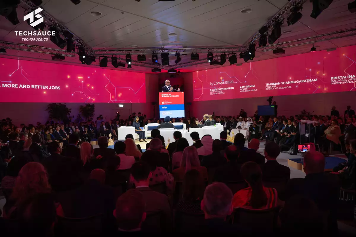
World Bank, IMF, and Singapore leaders explain how Small AI, simple tools that work even on a 3G phone, could help create jobs for 1.2 billion young people, and which sectors and p...
0
Cloudflare Field CISO Volker Rath says AI is weakening traditional defenses. Organizations need Zero Trust, security teams that act as engineers, policy written as code, and clear ...
0